
This is a side story in the "Black-Box Castle" series. The main chapters dealt with skills on paper—folding a network into two elements (Thévenin, Norton), winding a loop into equations (Kirchhoff), and splitting multiple sources into single ones (Superposition). This chapter changes the subject: the line of defense at the castle gate.
The formulas are the same, but the traps are not on paper. They hide in the fine print of datasheets, on package pins, and in that trace you assume is "only two millimeters anyway."
Story: The Gatekeeper of Thunderstorm Valley
North of the Black-Box Castle in Fog Valley lies a thunderstorm valley. Every summer, three kinds of water rush down the valley:
- A crack—an extremely short, violent jet of water—lasting one nanosecond, peaking at thirty amps. This is electrostatic discharge (ESD).
- A flood crest lasting a dozen-odd microseconds—rising to its peak in eight microseconds, falling to half in twenty. This is the 8/20 µs surge.
- Water flowing back through the bellows when the neighboring smithy shuts down—this is the half when a relay or solenoid de-energizes.
The castle gate originally had no gatekeeper. The door knocker was smashed three times, the bookkeeper's abacus was soaked twice, and once, three days after the rain stopped, the guard dog was still barking at empty air.
Grandpa Copper-Nail posted a rule by the gate: a gatekeeper stands at the door. Normally he dozes in his chair—reverse high impedance, leaking only a few nanoamps. The moment the water level at the gate crosses a certain mark, he jumps up, diverts all the water into the moat, and pins the gate's water level down. When the water recedes, he goes back to sleep.
This gatekeeper is called TVS (Transient Voltage Suppressor).
Here's the problem: the gatekeeper has three brothers, with completely different temperaments.
- The eldest (non-snapback): once he stands, he stays put, only slowly sitting back down after the water recedes. Steady as an old dog, but tall—the doorway needs a very high frame.
- The second (shallow snapback): when bumped, he crouches a little, then stands right back up.
- The third (deep snapback): one bump and he crouches all the way down, lower than anyone, so no wave can top the threshold. But once he crouches, if the water level at the gate is already higher than his head, he can never stand up again.
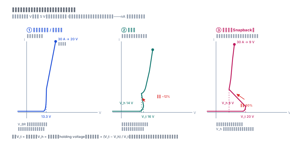
Figure 1: Snapback depth = . The eldest is "no snapback", the second "shallow snapback" (10%~20%), the third "deep snapback" (up to 40%~60%). Deep snapback gives the lowest clamping and the smallest capacitance, but once drops below the circuit's operating voltage, it loses even the freedom to turn off—Section 5 covers this in detail.
1. A TVS Is a Floodgate, Not a Current Limiter
Get the concept straight and you'll eliminate half of all selection mistakes:
A TVS does not destroy energy; it only routes energy to ground. It sits in parallel between the protected node and ground—high impedance normally, conducting the instant an overvoltage appears, stealing the surge current away from the chip. It has no "current limiting" ability at all—the surge current is pushed by the source, and the TVS can only decide how much it takes.
Three iron rules follow:
- It must be in parallel. Putting it in series is like installing a fuse for yourself—and the exploding kind.
- It must be close by, because there is inductance in the path (Section 6 will prove "1 mm = 30 V").
- There must be impedance or a disconnect device upstream (fuse, PPTC, current-limiting resistor, connector/cable inductance). Without impedance, the surge source is an infinite water tower—however much the TVS takes, it pours more.
Energy sharing is also a clean formula. Let the surge source open-circuit voltage be , the series impedance , and the TVS clamping voltage :
Note that ratio : the larger the series impedance, the more energy lands on the resistor and the easier life is for the TVS. That's why a 10 Ω series resistor lets a small SMB-packaged device survive a surge that would otherwise require an SMC package. Conversely, when approaches 0 (say, hanging directly on a battery), every bit of energy lands in the TVS's lap.
While we're at it, let's line up a few of the TVS's "colleagues" so you don't buy the wrong specialist:
| Device | Response | Current capability | Characteristics | One-liner |
|---|---|---|---|---|
| TVS diode | ps~ns | Medium | Precise clamping, repeatable, no aging | The fastest gatekeeper |
| MOV varistor | ns | High | Cheap, high energy, ages | A guard who eats well but wears out |
| GDT gas discharge tube | µs | Very high | Huge current, follow-current issues, limited life | Thor's hammer—each swing counts |
| Zener diode | µs | Low | High precision, low power | An old gatekeeper, only good for small thieves |
The TVS's strengths are fast + precise + no aging; its weakness is it can't swallow too much energy at once. That's why industrial sites commonly use a two-stage "GDT/MOV leads, TVS finishes" structure—that's Section 7's topic.
2. Reading the Curve: Six Parameters
90% of selection errors come from "only looking at the two numbers VRWM and VC." A reverse I-V curve actually holds six parameters.
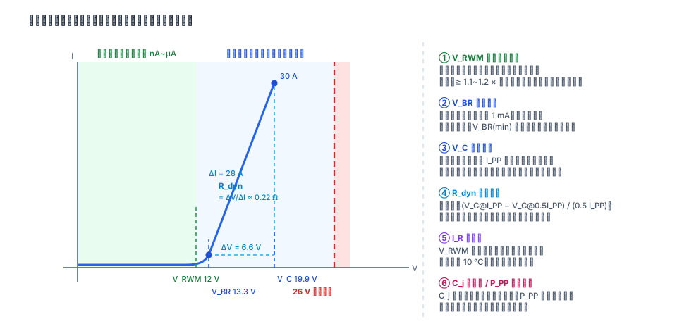
Figure 2: The green zone on the left is "normal operation, high impedance," the blue zone in the middle is "surge arrives, conduct and divert," and beyond the red line on the right is "the protected device's absolute maximum rating." The entire curve must stay left of the red line—that is the whole goal of selection.
| Parameter | Meaning | How to use |
|---|---|---|
| Reverse standoff voltage—the maximum DC voltage it can withstand long-term without conducting | maximum operating voltage | |
| Leakage current at | A must-check for battery devices; roughly doubles every 10 °C | |
| Breakdown voltage, measured at a specified test current (commonly 1 mA) | Look only at the minimum, and account for cold drift | |
| Clamping voltage, measured at the single point | Must be converted to your own current, see below | |
| Dynamic resistance—the slope after turn-on | ||
| Junction capacitance | Look at this for high-speed lines, see Section 8 | |
| Peak pulse power (usually specified at 10/1000 µs) | Only meaningful with the real waveform |
The third row is where people crash most often. A datasheet saying " V @ A" does not mean the line is always 19.9 V. The real clamping voltage is
Take a device with V and V @ 30 A: . If your surge is only 5 A:
Don't scare yourself with 19.9 V, and don't fool yourself with 13.3 V. The former is the "retail price at the 30 A moment," the latter is the "wholesale price at the 1 mA moment"—what you actually pay is the price in between.
Accuracy note: this linear formula has significant curvature near the breakdown region, so treat it as an engineering estimate. If you care, ask the vendor for a TLP curve or I-V plot instead of extrapolating from two points.
Temperature must be considered in two directions:
- has a positive temperature coefficient, roughly per degree Celsius. Breakdown voltage rises when hot (no false triggering), and is lowest when cold—so when checking " above maximum operating voltage," use the −40 °C point.
- grows exponentially, roughly "doubling every 10 °C." A device specified at 1 µA at 25 °C could be 30~60 µA at 85 °C. With a battery on standby for three months, this alone decides whether customers praise your product or return it.
3. Three Red Lines: Selection Is Squeezing a Window
The protected chip has only one hard limit: Absolute Maximum Ratings. The TVS's entire job is to ensure that during a surge, the voltage on the chip's pins never exceeds it.
Hence three inequalities that must all hold at once:
- ① ensures "no conduction in normal operation"—don't let the TVS leak, partially conduct, or heat up at normal voltage.
- ② ensures "the breakdown point is above the operating voltage," including cold drift—otherwise it breaks down the moment power is applied in winter.
- ③ ensures "it clamps during the surge"; the 0.8 leaves margin for temperature, lot-to-lot variation, and "that bit of inductance you didn't account for."
How wide the window is decides whether the device works. Let's run through a real 24 V industrial power rail:
- Nominal 24 V, ±10% → 26.4 V; switching ripple → 26.8 V; power-on overshoot 1 V → take the maximum operating voltage as 28 V.
- The protected Buck chip has an absolute maximum of 60 V.
- Measured surge (8/20 µs, with a PPTC and one meter of cable upstream): 5 A.
Put three candidates side by side and actually compute :
| Candidate | @ | Verdict | ||||
|---|---|---|---|---|---|---|
| SMBJ30A | 30 V | 33.3 V | 48.4 V @ 12.4 A | 1.22 Ω | 39.4 V | ① barely passes (30 vs 33.6), margin too thin |
| SMBJ33A | 33 V | 36.7 V | 53.3 V @ 11.3 A | 1.47 Ω | 44.1 V | ✓ all three lines pass |
| SMBJ36A | 36 V | 40.0 V | 58.1 V @ 10.3 A | 1.76 Ω | 48.8 V | ③ on the line (48 vs 48), too risky |
SMBJ33A's three red lines: (well, this one actually misses by 0.6 V—with 1.2 it fails, with 1.1 it passes. In this kind of "on the line" situation, go look up the chip's measured ripple instead of using estimates); ✓; ✓.
What if the Buck has a 40 V absolute maximum instead? Red line ③ becomes —instant failure. This is the truth behind so many "I installed a high-power TVS and the chip still blew up" stories: it's not that the TVS isn't trying; the window simply isn't wide enough. At that point there are only three paths:
- Make the surge smaller: add a 10 Ω series resistor / PPTC / ferrite bead to shave it first (remember to calculate the resistor's power dissipation);
- Go two-stage: GDT or MOV leads, TVS finishes, with decoupling elements in between;
- Switch to a bigger chip or a lower-clamping technology—but option 3 has a prerequisite on power rails, see Section 5.
Conversely, there's an even more fundamental path: swap in a DC-DC with V. Half of selection problems are on the TVS side; the other half come from choosing a protected device with specs that are too tight.
4. Energy and Junction Temperature: How Many Joules Can It Really Eat
Getting the voltage right doesn't mean it survives. A TVS basically dies of heat: short-term energy burns through the junction, or long-term average power pushes the junction temperature up.
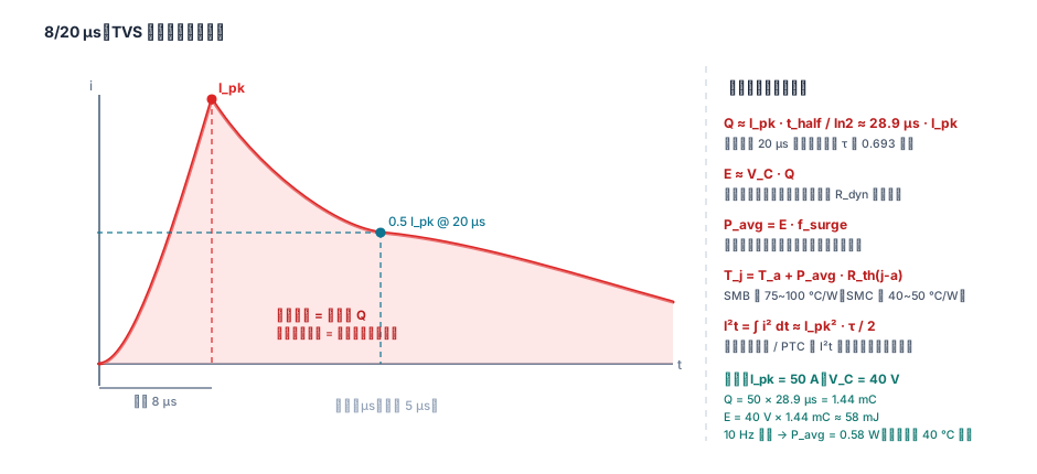
Figure 3: For 8/20 µs, "20 µs" means the half-value time, so the exponential tail's time constant is . Don't use 20 µs directly as τ, or your energy calculation will be 30% too low.
Four formulas, one per line:
Example: A, V.
- mC
- If this is a once-a-day event, is small enough to ignore and the "single-shot energy" is what matters;
- If this is a continuous 10 Hz surge, W, and with the SMB package's ℃/W, junction temperature rises 40~60 ℃—dangerous in summer.
Single events and repetitive events are two different worlds. The datasheet's is a single pulse; for repeated hits, look at the derating curve or simply calculate by . Many people read "can withstand 600 W" as "can eat 600 W continuously"—that's using a fire hose as a water main.
Fuse coordination is settled with —that's the referee for "who dies first":
In the example, . The design goal: during a normal surge, neither acts (the TVS blocks, the fuse doesn't blow); during a sustained fault, the fuse dies first—don't let the TVS hold on until it becomes a carbonized little block.
| Scenario | Energy | Who handles it |
|---|---|---|
| Relay/solenoid de-energizing, H, mA | mJ | Easy for a TVS; it doubles as a freewheeling path |
| ESD, IEC 61000-4-2 contact ±8 kV | mJ-level per strike, but 30 A / 1 ns | The TVS's home turf |
| 8/20 µs, 50 A, clamping at 40 V | 58 mJ | Comfort zone for SMB/SMC |
| Hot-plug, 1000 µF charged to 24 V | Not the TVS's job—use soft-start / hot-swap controllers |
The last row deserves to be carved into your desk: hot-plug inrush is a "long-duration, high-energy" event, not a surge. Asking a TVS to handle it is like asking a gatekeeper to block an entire river—he can hold back a moment, but not three milliseconds.
5. Deep Snapback vs Shallow Snapback: How Low the Gatekeeper Crouches
This is the hottest and most easily misbought category of recent years. Many domestic/Taiwanese vendors put it in the title as a selling point ("deep snapback", "Snapback", "ultra-low clamping"), but few selection guides spell out: why it can crouch this low, and what lets it stand back up afterwards.
Mechanism: After Avalanche, the Parasitic Transistor Takes Over
A normal TVS only has avalanche breakdown: when the voltage reaches , carriers multiply, current surges, and the voltage barely changes—that's the "no snapback" on the left of Figure 1.
Deep snapback adds one more layer of structure: there is a parasitic four-layer pnpn inside the device (essentially a small SCR). When avalanche current flows through the body resistance , it creates a voltage drop that forward-biases the parasitic NPN's emitter junction, so:
Once the positive feedback is established, the criterion is the classic thyristor turn-on condition:
Once satisfied, the device jumps from the "avalanche state" into a "low-impedance state," the voltage collapses to the holding voltage , and current can keep rising—that's the negative-resistance region where the curve bends back (right side of Figure 1).
The negative-resistance region also brings a hidden property: two deep-snapback devices in parallel on the same node will "fight for current"—the one that triggers first pulls the voltage down, and the other can never trigger. In multi-channel protection, don't expect them to share evenly.
Pros and Cons: One Table to See All Three Brothers
| Dimension | No snapback (avalanche/Zener) | Shallow snapback | Deep snapback |
|---|---|---|---|
| Curve | Monotonic rise after breakdown | Triggers, dips 10~20%, then rises | Triggers, plunges 40~60%, then rises |
| trigger point | Slightly above operating voltage | A "design point" clearly above operating voltage | |
| holding voltage | Slightly below | Far below (can go down to 2~8 V) | |
| Dynamic resistance | Medium | Medium | Low |
| High-current clamping | Highest | Medium | Lowest |
| Junction capacitance | Large (several pF to tens of pF) | Medium | Small (down to 0.3~0.5 pF) |
| Latch-up risk | None | Low | Yes, and it's a design-level risk |
| Temperature/spread | Good | Good | , spread widely, and sensitive to dV/dt |
| Datasheet data | Complete | Average | Often only typical curves; , may not be specified |
| Typical use | Power rails, automotive, industrial | General IO, low-voltage rails | High-speed data lines, ESD entrances |
One Criterion Decides Whether Deep Snapback Is Usable
The key isn't how low is, but who is powering this device, and how much they can supply.
The complete latch-up condition is both of these at the same time:
Here is the holding current—the minimum current that keeps the "" positive feedback from failing. It's typically in the 10~50 mA range, but unfortunately half of datasheets don't specify it.
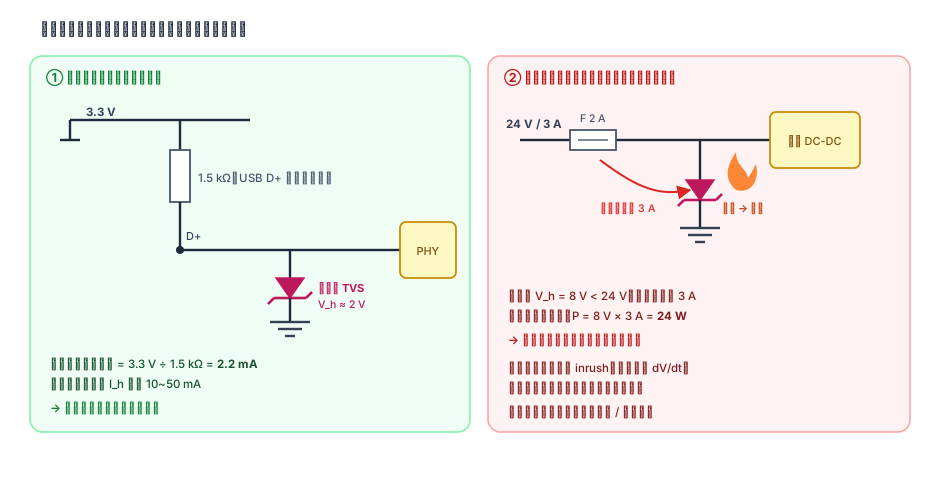
Figure 4: On the left, the deep-snapback TVS hangs on USB D+, and the 1.5 kΩ pull-up can only supply 2.2 mA—less than the holding current—so once the surge passes, it turns itself off. On the right, the identical device hangs on a 24 V/3 A power rail: V is below 24 V and the source can pump 3 A, so it gets pinned at 8 V × 3 A = 24 W until the fuse acts or it carbonizes itself.
Usable / Not Usable: a Scenario Checklist
| Scenario | Deep snapback | Why |
|---|---|---|
| USB 2.0 D+/D−, HDMI/Ethernet differential pairs | ✅ A must | Weak source (pull-up/termination resistors) + needs tiny + needs very low clamping |
| Sensor inputs, antennas, buttons, ADC front-ends | ✅ Good | High source impedance can't supply |
| 3.3 V / 5 V IO pins (CMOS push-pull drivers) | ⚠️ Use with care | The driver can supply tens of mA, possibly more than ; requires rail voltage |
| 5 V / 12 V / 24 V power rails | ❌ Don't use | Low-impedance strong source; triggering means latch-up |
| Direct battery nodes, charging ports, hot-swap entrances | ❌ Never use | Inrush di/dt lights it up first, then the source keeps supplying |
| Automotive 12 V/24 V, load-dump nodes | ❌ Don't use | Same as above, plus automotive specs require a monotonic curve with no negative resistance |
| AC 220 V input | ❌ | Needs bidirectional devices + high energy—that's MOV/GDT territory |
If you insist on using deep snapback on a "semi-strong source" (say, some IO pin), remember four amulets:
- must be higher than the node's maximum operating voltage, with 20%+ margin;
- Add a series current-limiting resistor so the source can supply at most ;
- Get , , and the -vs-dV/dt curves from the vendor—don't treat typical values as guaranteed ones;
- Verify power-on transients separately: soft-start dV/dt and hot-plug inrush are both "invisible triggers" for deep snapback.
Shallow Snapback: the Middle Child Nobody Advertises Loudly
Shallow snapback (only a 10~20% dip after triggering) has far less fame than deep snapback, but in engineering it's a very comfortable option:
- The curve is nearly monotonic, and the latch-up risk is low enough to ignore;
- Temperature and lot-to-lot spread are small, datasheets are complete, and you can safely write it into design rules;
- The price is higher clamping than deep snapback at high currents—on nodes like 3.3 V where "the window is only 1 V," it may fail to protect.
One sentence to summarize the three brothers: deep snapback is the highest-performing gambler, no snapback is the safest straight shooter, and shallow snapback is the middle option that can actually go to volume production.
6. Layout: One Millimeter of Trace Equals Thirty Volts
All the previous calculations rest on one premise: "the voltage the chip pin sees equals the TVS's clamping voltage." That statement holds in exactly one case: trace inductance is zero. In reality it isn't.
This is not fear-mongering; it's dimensional analysis. A 10 mm branch, two vias, and a narrow pad add up to 12~15 nH—an extra drop on the order of 400 V. The 44 V clamp you carefully calculated already reaches over four hundred volts at the chip pin.
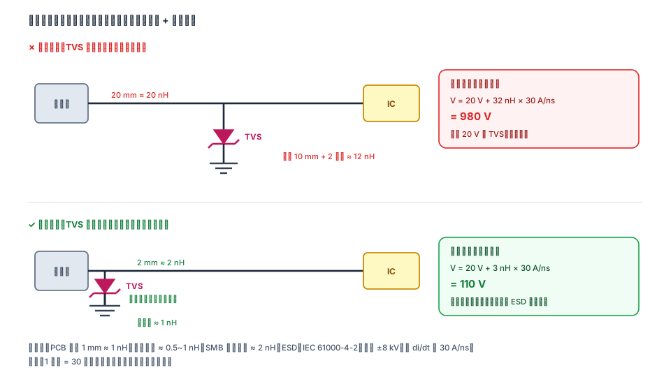
Figure 5: Note the line in the correct drawing—"Still high? That's why the chip's own on-die ESD protection can't be omitted"—the TVS is an outsourced bodyguard; the chip's internal ESD is the close-protection bodyguard. They don't replace each other.
Five layout rules—memorize them; they can save your life:
- Put the TVS at the connector, don't let the surge travel through 20 mm of trace before meeting it;
- Keep the ground return as short and wide as possible, put vias directly in the TVS's ground pad, don't route to the other end of the board;
- The protected trace must pass the TVS before entering the chip, the order can't be reversed (the trace should pass "through" the node, not branch off to it);
- Don't leave long stubs—a stub is an antenna plus an inductor;
- Be careful with shared grounds: the path surge current takes through the ground plane couples into other signals through common impedance.
A commonly ignored detail: where you measure decides what you see. Measure across the TVS and you're verifying the device; measure from chip pin to ground and you're verifying the design. The former always looks pretty; the latter decides whether the product survives.
7. Two-Stage Protection: Let the Big Guy Go First
When energy exceeds a single TVS's capability (lightning, long-line induction, AC entrances), split into two stages. The typical arrangement is "GDT or MOV + TVS," with a decoupling element in between—otherwise, in the few microseconds before the first stage conducts, all the pressure lands on the second stage.
The decoupling element is usually an inductor or a stretch of trace inductance that staggers the two stages' response times:
The selection order is back to front: first pin down what the chip can tolerate (), then set the second-stage TVS's clamping, then calculate how much the first stage must absorb, and only then the GDT/MOV's surge rating. Choose in reverse and you'll almost certainly crash.
8. Junction Capacitance: the Invisible Speed Limit on High-Speed Lines
in parallel with the signal line is like hanging a capacitor on the trace. It rounds off the rising edge:
is the parallel combination of the driver source impedance and the termination resistance. Rough rule of thumb: every time doubles, the eye height drops a notch and jitter ticks up. The approximate "tolerance ceilings" for common interfaces are:
| Interface | Speed | Recommended | Notes |
|---|---|---|---|
| USB 2.0 High Speed | 480 Mbps | < 3 pF | Match the differential pair |
| USB 3.x / HDMI 2.0 | 5~6 Gbps | < 0.5 pF | Deep snapback's home turf |
| Ethernet 1000BASE-T | 1 Gbps | < 3 pF | Watch pair-to-pair matching |
| RS-485 / CAN | ≤ 10 Mbps | < 50 pF | Much more forgiving |
| ADC front-end / sensors | DC~kHz | Doesn't matter | Can even double as a filter cap |
This is where deep snapback is truly irreplaceable: its low clamping is "performance," and its low capacitance is the "admission ticket." On these interfaces, a non-snapback device's can't even get through the door.
9. The Five-Step Process (Run Through Before Layout)
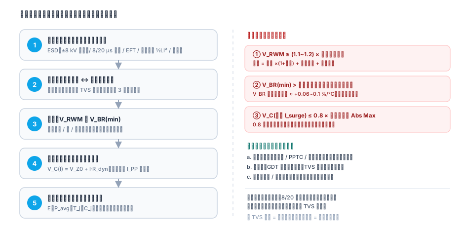
Figure 6: Order matters. Those who draw the threat diagram first finish selection in ten minutes; those who flip through selection tables first spend three days—and then it blows up.
10. Ten Crash Sites
All real sightings, sorted by how often people get bitten:
- Treating @ as the actual clamp. Your surge is only 5 A, yet you scare yourself with the 30 A price list—or the reverse, treating the 1 mA as the clamp and comforting yourself.
- Comparing the typical against the operating voltage. Look at the minimum, and factor in the −40 °C drift.
- Ignoring temperature's effect on leakage. Spec'd at 1 µA at 25 °C, it's sixty times that at 85 °C—battery standby current blows the budget across the board.
- Deep snapback on a power rail. One trigger, one burned device—and then you question your life choices.
- Measuring deep-snapback with a slow dV/dt source. The static curve looks great; the real trigger point is completely different.
- The TVS sitting 20 mm from the connector. The chip dies for no apparent reason—until you probe across the TVS and see it's "perfectly fine."
- Only a TVS, no upstream impedance. The whole surge lands on it, and the P-type package blows into an N-type.
- Using a TVS as OVP. Wire 48 V into a 24 V port by mistake and the TVS burns first, then the downstream follows. Sustained overvoltage needs an eFuse / hot-swap controller—a TVS only blocks transients.
- Mixing up bidirectional and unidirectional. A unidirectional TVS on an AC or bidirectional differential signal gives the surge a one-way street—the reverse direction takes everything.
- Forgetting the chip's own on-die ESD layer. Inner and outer layers form a series window—calculate them together, don't let them blame each other.
11. Quick Reference: Common Power Rails
| System | Suggested | Starting part | Notes | |
|---|---|---|---|---|
| 5 V | 5.5 V | 6.5 V | SMBJ6.5A (6.5CA if bidirectional) | For 5 V USB VBUS, confirm the upstream can current-limit |
| 12 V | 13.2 V | 15 V | SMBJ15A | Automotive 12 V must pass ISO 7637—separate calculation |
| 24 V | 28 V | 33 V | SMBJ33A | Narrow window; compute first |
| 48 V PoE | 57 V | 58~64 V | SMBJ58A | On the DC side, watch voltage rating and leakage |
| 3.3 V high-speed IO | 3.6 V | Deep-snapback only | 0.5 pF-class ESD array | Look only at and |
| 220 V AC | — | — | MOV + GDT + fuse | Don't let a TVS take it all |
Four Exercises for Yourself
- A 24 V industrial rail, maximum operating voltage 28 V, the protected LDO's absolute maximum is 36 V, and the measured surge is 8/20 µs at 8 A. Work it out: can a single SMBJ33A hold? If not, what parameters do the three remedy paths need? (Hint: V, V—far apart; the easiest moves are adding a series resistor or switching to a 60 V-rated device.)
- A deep-snapback TVS with V, V, mA. What happens if it's hung on a 5 V/1 A supply? What about on a 5 V signal line through a 10 kΩ pull-up? Write out the current and power for each.
- A 1.5 pF TVS on a 480 Mbps differential pair, , original ns. Calculate the degraded rise time, and explain why HDMI 2.0 requires a 0.5 pF device.
- 8/20 µs, A, clamping 30 V, twenty times a day. Compute , , and decide whether an SMB ( ℃/W) is enough. If not, would you change the device or the architecture first?
The Tail
One-sentence summary: the gatekeeper's job has three parts—stay still in normal times ( and ), don't let visitors slip in ( and ), and don't linger afterwards ( and ). Add one rule that runs through the whole article: don't let him stand too far from the gate (1 mm = 30 V).
As for deep snapback, it's not mysterious and not a scam—it simply trades "performance" for "dependence on the source." On a weak source, it's a genius; on a strong source, it's a time-bomb resistor. There is only one test: after that device crouches down, who has the power to pull it back up?
Sister articles: Thévenin's Theorem · Norton's Theorem · Kirchhoff's Laws · Superposition Theorem · Femtoamp Current Measurement · MOSFET Parameter Quick Reference