
This is a hands-on record outside the "Black Box Castle" series. The earlier pieces dealt with Thévenin, Norton, Kirchhoff, and Superposition on paper; this one changes the subject: how to turn a current as small as 10⁻¹⁵ A into a voltage that an oscilloscope or ADC can actually read. There aren't many equations, but there are plenty of traps.
Story: The Dew Ledger of Fog Valley
Deep in Fog Valley there is a well, and the dew condensing on its walls forms an extremely thin trickle of water. The little fox Ali has to figure out: exactly how many drops of water fall per second.
It tried three methods, and all of them failed:
- Catching it in a measuring cup: after a full day, the bottom of the cup still didn't look wet.
- Driving a water wheel: the flow couldn't turn the wheel; instead it was pushed back by the wheel's own resistance.
- Sticking a leather tube into the well mouth to measure the pressure difference: most of the water seeped away through the cracks in the tube wall, and what was measured was only a fraction.
Grandpa Copper Nail said: your mistake is "making the water adapt to your measuring instrument." What you should actually do is three things—
- Station a gatekeeper to hold the water level in the bucket firmly at the 0 mark. If the level doesn't move, the water in the well feels no "back pressure" and is willing to give up all of it;
- If the gatekeeper wants to hold the level at 0, he has to force the water out through a very long, very thin tube. The thinner and longer the tube, the greater the pressure difference the same flow requires—read the pressure difference, and you've read the flow;
- Dig a moat around the bucket, with the water level in the moat moving together with the bucket. With no height difference, the seepage can't get in.
The gatekeeper is the op amp, the long thin tube is the feedback resistor , and the moat is the guard ring on the PCB. All the remaining work is making sure these three things don't sabotage each other.
1. How Heavy Is What This "Scale" Has to Weigh
First lay out the orders of magnitude, otherwise everything that follows is empty talk.
Six thousand electrons per second. That sounds like a lot, but spread across the leakage of an entire chip, the dark current of a photodiode, or the ion flow of a pH electrode, it is just a tiny offset next to the background noise.
Another angle makes it more intuitive—using the current to charge a capacitor:
1 fA charging 1 pF raises the voltage by only 1 mV per second. Any one-millimeter trace you never noticed, as long as its surface resistance is , can leak 1 pA under a 1 V difference—1000 times larger than the signal you want to measure.
Common fA-level scenarios are actually all around you:
| Scenario | Typical current | What's hard |
|---|---|---|
| Photodiode (low light, CT detector) | 1 fA – 10 nA | Dynamic range + junction capacitance |
| Ionization chamber / semiconductor detector | 0.1 fA – 1 pA | Cable leakage, microphonics |
| pH glass electrode, ion-selective electrode | 1 pA – 1 nA | Source resistance up to 10⁸–10⁹ Ω |
| Chip standby leakage, capacitor leakage | 1 fA – 100 pA | The fixture's own leakage is larger than the DUT |
| Electrometer / mass spectrometer Faraday cup | 0.1 fA – 1 pA | Everything (this is the hardest) |
2. The Gatekeeper Takes the Post: Why a Transimpedance Amplifier Turns Current into Voltage
Holding the Water Level Steady = Virtual Ground
Wire the op amp like this: the inverting input connects to the signal source (photodiode/electrode), the non-inverting input is grounded, and the feedback network is (with a small capacitor in parallel).
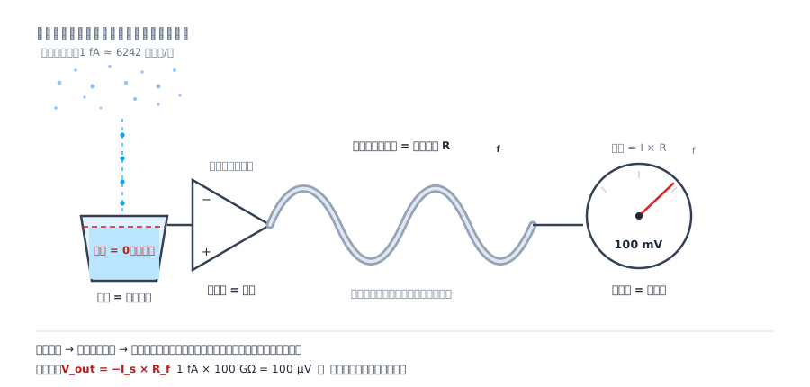
Figure 1: The gatekeeper doesn't need to "block" the water; he only needs to keep the water level still. When the level doesn't move, there is no back pressure in the well, so the water is willing to come over entirely; and to keep the level still, he must force the water out through the tube—the greater the pressure difference, the greater the flow.
The op amp drives its output hard so that . This state in which "the inverting input is pinned at 0 V" is called a virtual ground. Writing KCL at the summing node (taking as the signal current flowing into the node; arrow direction in Figure 2):
The minus sign is purely a direction convention. Draw the arrow the other way and the sign flips; the physics is unchanged.
This single equation is the entire principle. 1 fA times 100 GΩ gives 100 µV; times 1 TΩ gives 1 mV. Pick to match the output swing you need.
The Biggest Gift of the Virtual Ground: The Source Isn't "Stolen From"
Many people's first reaction is "can't I just put a resistor in series and measure the voltage drop?" No—and it fails badly.
Assume the source's shunt resistance is (a photodiode's shunt resistance, or a pH electrode's internal resistance, are both in the GΩ class), and you insert a sampling resistor :
If and you use a multimeter's 10 MΩ range to measure the drop, the source will only give you 1% of its current. The other 99% slips back through the source's own internal resistance.
With a virtual ground, the voltage across is always 0, so it can't steal a single electron:
It's the same formula, but replace with the "0 Ω" clamped by feedback and the error disappears. That's why every electrometer, picoammeter, and source-measure unit's current range is an op amp plus a big resistor inside.
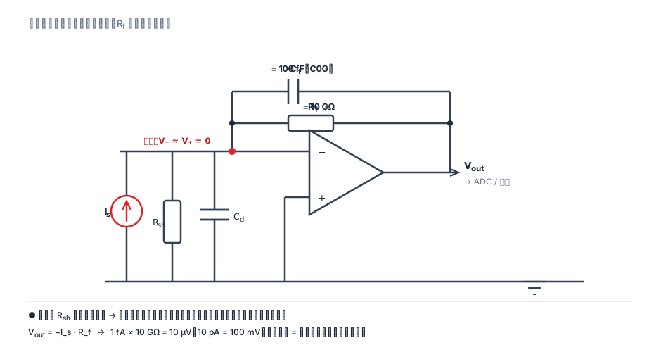
Figure 2: and hang right on the summing node, but the virtual ground means there's no voltage difference across (no current stealing); still slows the bandwidth—together with it sets the time constant.
Bandwidth: The Tube's Thickness Decides How Fast You Can Read
where (source capacitance + op amp input capacitance + strays). The moment grows large, bandwidth drops in a straight line—that's the hardest physical constraint of the transimpedance method, not a question of design skill.
As a side note, the settling time (to 0.7% at ):
With 1 GΩ and 5 pF, and it settles in 25 ms; go to 100 GΩ and it takes 2.5 s to stabilize. This is why instruments that measure femtoamps always read so slowly.
Stability: That Tube Needs a "Damping Hole"
The formula above has a trap: introduces a pole in the feedback loop, making the loop cross 0 dB at −40 dB/dec with phase margin approaching zero—without it will ring or even oscillate. provides a zero that flattens the noise-gain plateau.
Engineering criterion (45°–60° phase margin):
Work an example: , , :
28 fF is too small, so in practice use 100 fF–1 pF. Note that here , so the bandwidth is barely eaten—this capacitor buys stability, not bandwidth.
The reverse view matters too: the larger the GBW, the smaller the minimum needed; an op amp with too little GBW forces larger, and bandwidth takes another cut. When selecting parts, GBW should be at least two orders of magnitude above the "pole set by ".
3. Choosing : A Resistor You Can Buy, Solder, and Keep Stable
Transimpedance gain is conventionally expressed in dBΩ: .
But output is only about "big enough"; what determines resolution is noise and bandwidth. This table puts the three together (, ):
| Output for 1 fA | Johnson noise | dB bandwidth | settling | 3σ minimum detectable at 1 Hz | |
|---|---|---|---|---|---|
| 1 MΩ | 1 fV | 129 fA/√Hz | 32 kHz | 25 µs | 390 fA |
| 10 MΩ | 10 fV | 40.7 fA/√Hz | 3.2 kHz | 250 µs | 122 fA |
| 100 MΩ | 0.1 µV | 12.9 fA/√Hz | 318 Hz | 2.5 ms | 38.7 fA |
| 1 GΩ | 1 µV | 4.07 fA/√Hz | 31.8 Hz | 25 ms | 12.2 fA |
| 10 GΩ | 10 µV | 1.29 fA/√Hz | 3.18 Hz | 250 ms | 3.9 fA |
| 100 GΩ | 100 µV | 0.41 fA/√Hz | 318 mHz | 2.5 s | 1.2 fA |
| 1 TΩ | 1 mV | 0.129 fA/√Hz | 31.8 mHz | 25 s | 0.39 fA |
This table is the whole truth about part selection: to get lower noise you can only raise ; raise and bandwidth and speed fall off a cliff. "Design" means finding the acceptable point among the three.
Four Hidden Traps of High-Value Resistors
- Voltage coefficient (VCR): put 1 V across a 100 GΩ thick-film resistor, then 10 V, and the value can differ by tenths of a percent to several percent. The fix is to stack several in series; each sees a smaller voltage and the VCR immediately improves by an order of magnitude.
- Temperature drift: ±100 ppm/°C is common; on 1 GΩ that's 0.1 MΩ/°C. It looks like only 0.01%, but the transimpedance gain drifts right along with it—long-term DC measurements require temperature control or periodic self-calibration.
- Moisture: high-value resistor packages aren't hermetic. When humidity rises, surface leakage creeps along the resistor body and effectively shunts a small resistor in parallel—the reading will only keep reading high. Conformal coating or sealing is mandatory.
- Mechanical stress / piezoelectric noise: high-resistance bodies are sensitive to deformation; a board vibrated slightly by a fan can show low-frequency wobble at the output. Mount it suspended on soft leads, and don't leave it hugging the board to be stretched by thermal expansion.
The T-Network: A Stand-in When There's No 1 TΩ Resistor
Three resistors in the 10 MΩ class can make an "equivalent 1 TΩ". The cost: the equivalent gain comes from resistor ratios rather than one stable high-value body, the noise gain increases, and it's extremely sensitive to leakage on . I only use it when a high-value resistor isn't available and numbers must come out immediately; for real instrumentation, one properly mounted glass-glaze 100 GΩ is far more reassuring.
4. Noise: The Tank Sloshes on Its Own
However diligent the gatekeeper, the tank itself will slosh. The resolution limit of femtoamp measurement is essentially set by three things.
1. Johnson Noise of the Feedback Resistor (The Floor)
(at 300 K). 1 GΩ gives ; 100 GΩ gives .
From this comes the minimum detectable current (, bandwidth ):
Note that it has nothing to do with the signal—it depends only on and bandwidth. To double the resolution, either multiply by 4 or divide the bandwidth by 4.
2. Op Amp Voltage Noise Through the Input Capacitance
The op amp's becomes an equivalent input current noise through :
Wait, the original formula is: $$i_{n,e}=e_n\left|\frac{1}{R_f}+j2\pi fC_{in}\right|\ \approx\ e_n\cdot 2\pi f C_{in}\quad(f\ \text{较高时})$$ — I'll translate properly below.
Actually let me write this section cleanly.
It rises with frequency. Take and : at 1 kHz it's , just 1/18 of the Johnson noise; it won't catch up to the 4.07 fA until 18.5 kHz. In other words, in narrowband femtoamp measurements this curve hasn't even lifted its head.
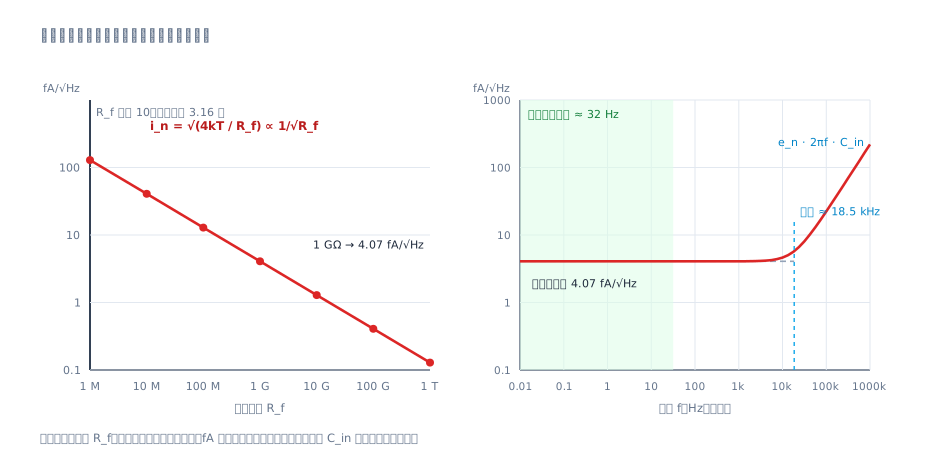
Figure 3: The slanted line on the left is —the only noise you can improve by adding resistance; the right side shows that is usually irrelevant in femtoamp-level, narrowband scenarios, unless you lower for speed and push the bandwidth above the kHz range.
3. Op Amp Current Noise and Shot Noise
The last term is the signal's own shot noise (the quantum limit): at 1 pA it's about ; at 1 nA it's 17.9 fA/√Hz. The larger the signal, the more it dominates—at that point stop agonizing over the op amp; you've hit the physics ceiling.
A Counterintuitive Conclusion: The Floor Is the Ceiling
Rewrite the Johnson formula to see "how much resistance is needed to measure 1 fA":
To get with , you need . Want to measure 100 aA? has to go to 1.5 TΩ—available to buy, but not solderable; the leakage exceeds the signal, and any temperature change makes it drift.
So the engineering boundary is clear: use the transimpedance method for DC femtoamps; below 100 aA, switch to the integration method or modulation (Section 9 below).
5. Choosing the Op Amp: Five Gates
Part selection isn't "whose is rated lowest"; it's about screening through the gates one by one. My own order:
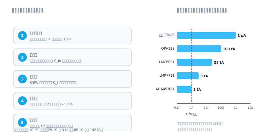
Figure 4: The chart on the right makes it obvious at a glance "why a general-purpose op amp won't work"—its bias current is three orders of magnitude larger than the signal you're trying to measure.
Gate One: and Its Drift
Every 10 °C rise doubles the bias current. An op amp rated 3 fA at 25 °C becomes 192 fA at 85 °C; add self-heating on top and you understand why electrometer input stages get their own thermal isolation, even a temperature-equalizing copper block.
Two easily missed points:
- varies with common-mode voltage. The "3 fA" in the data sheet is usually measured at some particular . Either run the input stage near the supply midpoint, or use bootstrapping to lift both ends of the source together, and only then will stay stable.
- Look at max, not typ. Design from the maximum value in the data sheet, and check the column across the full temperature range.
The acceptance criterion is simple: and its drift across the operating temperature should be less than 1/10 of the target current. If you can't meet it, you must calibrate (see Section 8).
Gate Two: Noise (, , )
In narrowband femtoamp scenarios, is often not the bottleneck; is the stealthy one: the larger , the harder stability becomes ( must grow), the narrower the bandwidth, and the earlier the corner of . Choosing an op amp with small is a better deal than choosing one with a whole 1 nV lower.
Gate Three: GBW and the Feasibility of
Run the Section 2 formula: if the computed is so small that "PCB stray capacitance is bigger than it", that op amp won't work—your circuit will oscillate according to the stray capacitance. As a rule of thumb, is reasonably safe.
Gate Four: Leakage—Package, Pins, ESD Diodes
- Package: SOIC/DFN are easier to work with than SOT-23, but what really decides leakage is pin spacing and the surface resistance of the package material. Use a large package whenever you can.
- ESD protection diodes: almost every op amp has them on the inputs. Their reverse leakage is pA-class at room temperature and even worse under light. So: never add external clamp diodes to the input; and don't expect diode protection to coexist with femtoamp accuracy.
- Photoelectric effect in plastic packages: the die in a plastic package responds to ambient light. Putting the board in an opaque box, or taping over the op amp with black tape, is the real answer to "why does the reading keep jumping" for many people's first femtoamp measurement.
Gate Five: Miscellaneous
and its drift (in a TIA it's mainly a DC offset that can be subtracted, but the drift can't), 1/f noise, output swing (with large the output may need to reach ±several V), single vs. dual supply, and whether there's a built-in guard-ring buffer (the ADA4530-1 integrates one—one less part, and one less leak).
Candidate Parts (typical values, order-of-magnitude reference; select from the latest data sheet maximums)
| Part | Input stage | (typ, 25 °C) | GBW | Suitable current range | |
|---|---|---|---|---|---|
| General-purpose CMOS (OPA320 class) | CMOS | ~0.5 pA | 8.5 nV/√Hz | 20 MHz | ≥ 1 nA |
| OPA129 | Difet | ~100 fA | 25 nV/√Hz | 1 MHz | ≥ 10 pA |
| LMC6001 | CMOS | ~25 fA | 22 nV/√Hz | 1.3 MHz | ≥ 1 pA |
| LMP7721 | CMOS | ~3 fA (max 20 fA) | 6.5 nV/√Hz | 17 MHz | ≥ 100 fA |
| ADA4530-1 | CMOS | ~1 fA (max 20 fA) | 14 nV/√Hz | 2 MHz | ≥ 10 fA, built-in guard-ring buffer |
One thing to note from this table: every order of magnitude lower in raises both the price and the difficulty by a step. Going from 1 pA to 10 fA is a part swap; going from 10 fA to 1 fA means changing your entire design habit (board, cleaning, shielding, temperature control).
6. Layout: Holding That One Square Millimeter
On the schematic, the summing node is just a little dot. On the PCB, it's the most fragile square millimeter on the whole board: it's exposed simultaneously to leakage, moisture, thermal EMF, electromagnetic fields, and light. Every formula above assumes that this square millimeter is clean.
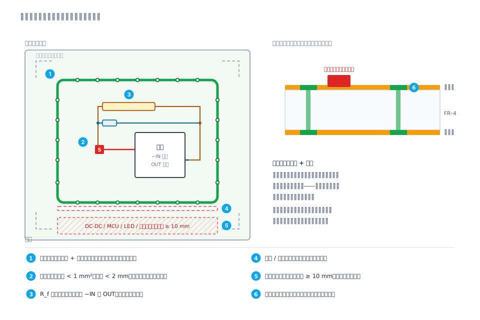
Figure 5: Three layers of defense—the ring (the guard absorbs the voltage differences on itself), the slot (cutting off the surface creepage path for leakage), and the cage (a shield against electric fields and light).
1. The Guard Ring: Give Leakage "No Height to Fall"
The principle is plain: leakage current = voltage difference ÷ surface resistance.
Ring the input node with copper and drive it to the same potential as the input node with a buffer (the buffer's input comes from the non-inverting input or the summing node). Then:
- From outside (5 V digital lines, 3.3 V supplies) to the guard ring: the voltage difference is still 5 V, but the current is swallowed by the low-impedance buffer and never reaches the summing node;
- From the guard ring to the input node: the voltage difference becomes the buffer's offset voltage, about 100 µV.
That's the theoretical value; in practice, limited by the ring spacing, board cleanliness, and humidity, getting – is already very good.
Specific drawing rules:
- Two layers: one on top, one on the bottom, with stitching vias every 3–5 mm along the ring to tie the two layers to the same potential (which also serves as an equipotential surface for the electric field).
- Ring width 0.3–0.5 mm, with around 0.5 mm spacing from the input pads.
- Put nothing inside the guard ring: no ground pour, no power, no digital signals; the ground plane starts outside the ring.
- The buffer itself must be a low-, low- op amp (an LMP7721 as a follower is the common choice), otherwise the ring's offset voltage will hand back everything you just saved.
2. The Input Node Itself: The Smaller and "Cleaner", the Better
- Keep the total pad + trace area within 1 mm², with trace length < 2 mm.
- No vias, no test points, no silkscreen marks. A via is a leakage path; a test point is an antenna.
- Place no decoupling capacitors, LEDs, relays, or DC-DC converters near the op amp's input pins.
- Mount the feedback resistor suspended (leads not touching the board), or upside down on the shortest path between the input and output pins; the ground plane beneath it must be cut away.
3. Moisture: The Cheapest and Deadliest Cut
FR-4's surface resistance collapses with humidity. With 1 mm spacing and 1 V across it:
| Relative humidity | Surface resistance (order of magnitude) | Leakage current |
|---|---|---|
| 20% | 10¹⁵ Ω | 1 fA |
| 40% | 10¹³ Ω | 100 fA |
| 60% | 10¹¹ Ω | 10 pA |
| 80% | 10⁹ Ω | 1 nA |
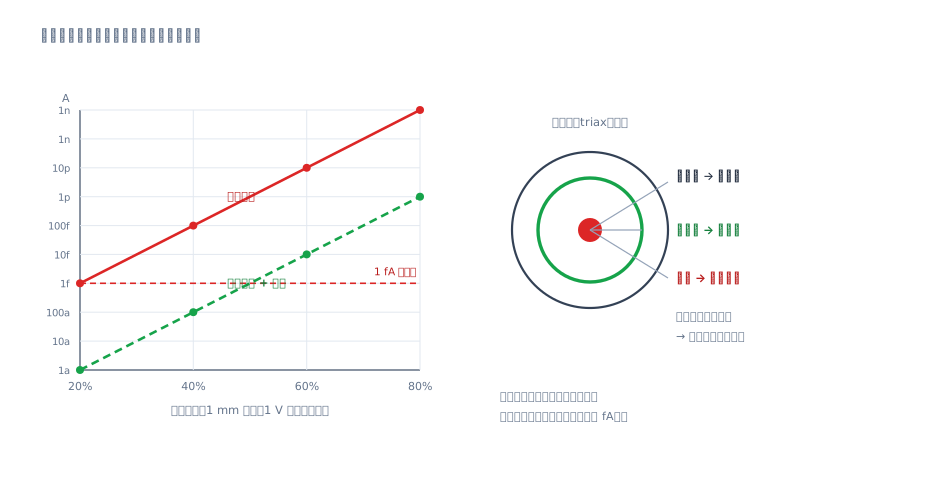
Figure 6: The left side explains why measurements are accurate in an air-conditioned room in winter, yet drift the moment you open a window in summer; the right side explains why ordinary coax can't be used at femtoamp levels—its dielectric is exactly that 10¹¹ Ω.
Countermeasures, ranked by cost-effectiveness:
- Use the guard ring first (free, biggest effect);
- Dry: a sealed box + desiccant, or fill the box with dry nitrogen. This is standard equipment on old electrometers;
- Clean: after soldering, wash with isopropyl alcohol + ultrasonic, and never use no-clean flux—flux residue, once it absorbs moisture, is a semiconductor that can hand you tens of MΩ of leakage;
- Conformal coating: it blocks moisture, but watch its volume resistivity and piezoelectric effect; in ultra-high-resistance situations I'd rather "dry + shield" than coat blindly.
4. Thermal EMF: 1 µV Equals 1 fA
Any junction of dissimilar metals is a thermocouple. Copper–solder is about 1–3 µV/°C; copper–Kovar and copper–copper oxide can reach 10–40 µV/°C. A 0.5 °C temperature difference on the board can pile up several µV.
And through a 1 GΩ transimpedance:
One microvolt of thermal EMF equals exactly one femtoamp of false signal. This is why your reading slowly drifts when "someone walks by," "the AC vent swings over," or "a finger nears the board."
What to do:
- Lay out the input area symmetrically so the two thermocouples cancel back-to-back (same metal, same length, same width);
- Keep the input area away from power devices, away from board edges, and away from fans;
- Add a shield (a metal box that doubles as an isothermal cover, tied to analog ground); if you can, wrap the op amp and together in a temperature-equalizing copper block;
- Keep pad finishes consistent: don't have ENIG on one side and tin plating on the other.
5. Cables: Ordinary Coax Won't Do
- The inner dielectric of ordinary coax (PVC/PE) has finite volume resistivity, and when flexed it also exhibits the triboelectric effect—one bend is tens of fA of current spikes;
- The correct approach is triax: inner conductor = signal, inner shield = guard, outer shield = chassis ground. With no voltage difference between the inner conductor and inner shield, leakage is collected by the inner shield;
- For higher demands use low-noise cable (with a graphite-coated core to suppress triboelectric effects);
- Connectors should be coax/triax too; no header pins or Dupont wires—those are antennas and leakage paths.
6. Power and Interference
- Don't power the analog front end from a DC-DC converter; switching noise couples in through the supply and through space. Use a linear regulator or a battery. Battery-powered noise-floor testing is the fastest way to hunt down interference.
- Connect digital and analog ground at exactly one point, near the ADC's or op amp's ground pin; don't let digital return currents pass beneath the input area.
- Suppress 50/60 Hz interference with shielding + short traces + integrating over integer multiples of the power-line period. In narrowband measurements, set the integration window to an integer multiple of 100 ms and the line frequency is eaten by the sinc nulls.
7. Error Budget: Write Every Term as a Current
After the design you must run a budget, otherwise you won't know which part of the reading is real. Example: target 0.1–50 pA, , , op amp ADA4530-1.
| Error term | Referred to input current | Note |
|---|---|---|
| Johnson noise (2.6 Hz bandwidth) | 2.1 fA rms | Cannot be eliminated; only raise or reduce bandwidth |
| Op amp | ~0.1 fA | Usually negligible |
| 0.0014 fA | ||
| (2.6 Hz) | ≈0 | Corner is above the kHz range |
| (max 20 fA) | 20 fA | Must be calibrated, otherwise it's the dominant error |
| temperature drift (ΔT=5 °C) | ~5 fA | Temperature control or periodic self-cal |
| Guard ring residual leakage | ~1 fA | Acceptable below 60% RH |
| Thermal EMF 2 µV | 0.2 fA | Referred as |
| tolerance 1% | — | A one-time calibration suffices |
Conclusion: the noise is only 2 fA, but the bias current is 20 fA. So the key to this meter isn't swapping the op amp—it's a zero calibration before every measurement (disconnect the input, or connect a shielded dummy load, and record the output). After calibration, a 10 pA signal can reach accuracy on the order of 0.05%.
8. Calibration: No Standard Source Needed—Use
- 1 pF + 1 V/s = 1 pA
- 1 pF + 1 mV/s = 1 fA
How: a 1 pF C0G/NP0 capacitor (or polystyrene, Teflon), one end on the summing node and the other on a slow ramp voltage (a DAC or integrator output, with a resistive divider). The ramp must be slow, monotonic, and clean—built with a battery and DAC, far better than a signal generator.
Two more free self-checks:
- Open-circuit method: disconnect the input completely (floating but still surrounded by the guard); the drift you read is your "system floor"—the sum of leakage + thermal EMF + noise.
- Short-circuit method: short the input to the guard; the reading should return near zero, and the part that won't return is + offset.
9. Below the Femtoamp: Integration and Modulation
Resistive transimpedance gives out below 100 aA. Two alternative routes:
The integration (charge) method:
1 fA × 1 s ÷ 1 pF = 1 mV. Its noise floor isn't Johnson noise but reset noise:
At 1 pF, —referred to a 1 s integration time that's 64 aA. An order of magnitude better than the transimpedance limit; the cost is that you must reset periodically (or use dual-slope) and deal with dielectric absorption.
Modulation / chopping: chop the light source, or modulate the bias with a square wave, and detect at kHz with a lock-in amplifier. Offset, thermal EMF, and 1/f noise are all moved out of band, leaving only the noise near that one spectral line. The equivalent bandwidth can reach the mHz range.
The price is time. Take (4.07 fA/√Hz) as an example; to pull 1 fA out of the noise (3σ):
| Noise density | Averaging needed to resolve 1 fA at 3σ | |
|---|---|---|
| 1 GΩ | 4.07 fA/√Hz | ~75 s |
| 10 GΩ | 1.29 fA/√Hz | ~7.5 s |
| 100 GΩ | 0.41 fA/√Hz | ~0.75 s |
This is why electrometers routinely take tens of seconds per reading. It isn't the instrument being slow; physics requires you to wait.
10. Checklist (Run Through Before Every Layout)
- Set first: use the "gain, noise, bandwidth" three-column table; don't guess.
- Compute with ; use C0G/NP0 or polypropylene for , never X7R/Y5V.
- The max value of must be less than 1/10 of the target current; otherwise design a calibration procedure.
- Input node area < 1 mm²; no vias, no test points.
- Guard ring on two layers + stitching vias, driven by a low- buffer.
- No ground pour inside the guard ring; the ground plane borders the ring from outside.
- suspended or upside-down, with the ground plane beneath it cut away.
- Digital/power areas > 10 mm from the input area, with a milled slot between them; the shield ties to analog ground.
- Clean after soldering; no no-clean flux; measurement environment humidity < 50%.
- Power-up order: first look at open-circuit noise (the floor), then connect the source; when the reading drifts, suspect thermal EMF and humidity first, not the op amp.
Small Exercises I Set for Myself
- You want to measure a 10 pA low-light current with a 10 Hz bandwidth using 1 GΩ. Calculate the rms Johnson noise and the relative error; then redo it with at 100 GΩ and state what you gave up. (Hint: 4.07 fA/√Hz × √10 ≈ 12.9 fA, i.e. 0.13%; with 100 GΩ the bandwidth is squeezed to 0.32 Hz and the noise drops to 0.41 × √0.32 ≈ 0.23 fA, i.e. 0.0023%—you gave up speed, range, and settling time.)
- A 3.3 V digital trace runs 0.5 mm from the input pin of a plastic-packaged op amp, and the board has sat in a 70% RH environment for three days. Estimate the order of magnitude of the leakage current, and give two remedies that don't change the board.
- What happens if you reduce from 100 fF to 10 fF? Explain using noise gain and phase margin (hint: moves up, the noise-gain plateau rises, and the slope when crossing 0 dB becomes −40 dB/dec).
Tail
The whole article in one sentence: the gatekeeper pins the water level (virtual ground), the long thin tube turns flow into pressure difference (), and the moat keeps leakage out (guard). Everything else—noise, bandwidth, thermal EMF, humidity—is a byproduct of these three.
There are really only three equations: , , . Remember these three, hold that one square millimeter, and all that's left is patience.
Sister articles: Thévenin's Theorem · Norton's Theorem · Kirchhoff's Laws · Superposition Theorem · First-Order RC Filtering · MOSFET Parameter Quick Reference